A diversity of people and ideas. coupled with free and open discourse, lays the foundation
27.Sep.1917
PCB Design Workshop
The PCB Design Workshop, organized by the IEEE Student Branch BITM and IEEE CAS BITM, was held from October 27th to 29th, 2025, at the Seminar Hall, Department of EEE, BITM. The resource persons for the workshop were Prof. Megha M Veerkar, Sumalatha B, Akhil Sai Mamidala, Sai Charan Teja Takkellapat, and Palem Venkata Sreenivas Reddy. The program was coordinated by Dr. Abdul Lateef Haroon P S, IEEE Branch Counsellor, BITM.
This three-day workshop was designed to provide participants with a comprehensive understanding of printed circuit board (PCB) design, fabrication, and testing—bridging theoretical foundations with practical industry-relevant skills. It aimed to enhance students’ knowledge of modern electronic systems by demonstrating how PCBs form the backbone of nearly all electronic devices, offering both mechanical stability and reliable electrical connectivity among components.
The workshop commenced with an overview of the significance of PCBs in electronic circuit design, highlighting their advantages such as compactness, reliability, ease of assembly, and signal integrity improvement. Participants explored various types of PCBs—single-sided, double-sided, and multilayer— along with their real-world applications ranging from simple LED modules to complex embedded systems.
The sessions also familiarized students with essential electronic components including resistors, capacitors, transistors, ICs, and diodes, emphasizing component placement, footprints, and layout design rules. A major highlight of the workshop was the hands-on training in KiCad, an open-source electronic design automation (EDA) tool, where participants learned the complete PCB design workflow—from schematic creation and component placement to routing and the generation of Gerber files for manufacturing.
The practical component of the workshop introduced participants to the fabrication and assembly stages of PCB production. Students gained first-hand experience transferring PCB layouts onto copper-clad boards, performing chemical etching to remove excess copper, and drilling holes for component insertion. Following fabrication, they learned proper soldering techniques, focusing on temperature control, solder joint quality, and troubleshooting common assembly errors. Each participant successfully fabricated and assembled a functional circuit, translating theoretical concepts into a tangible outcome.
Advancing to professional-level design practices, the workshop addressed advanced PCB design principles and industry standards. Participants were introduced to design parameters such as track width and spacing, routing optimization, signal integrity, EMI/EMC mitigation, and thermal management strategies. The importance of Design for Manufacturability (DFM) was emphasized to ensure reliability and ease of large-scale production. Students also worked through a practical case study involving voltage-level conversion circuits (5V to 3.3V), simulating real-world design challenges and reinforcing their understanding of best practices.
The workshop concluded with insights into industry workflows, including design validation, testing procedures, and the quality control standards followed in professional PCB manufacturing environments. Through interactive discussions and demonstrations, participants gained awareness of the skills required in the electronics and embedded hardware domains.
Workshop Outcomes
By the end of the workshop, participants were able to:
Understand the complete PCB design and fabrication process—from schematic creation to testing.
Use KiCad for schematic design, component placement, routing, and Gerber file generation.
Gain practical exposure to PCB fabrication and soldering techniques.
Apply advanced design concepts including signal integrity, EMI/EMC control, and DFM principles.
Identify and troubleshoot common design and assembly issues.
Develop confidence to undertake small-scale hardware projects independently and explore careers in electronic hardware design and manufacturing.
Related Events
25.Nov.2024
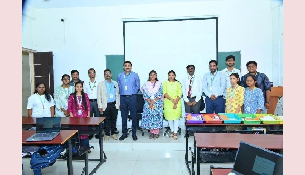
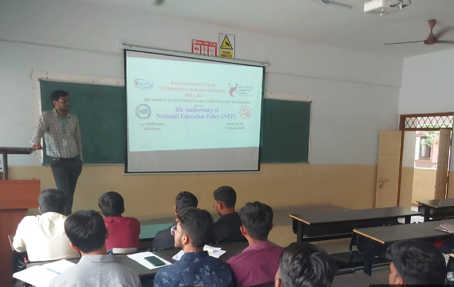
4th anniversary of the National Education Policy (NEP)